High piezolectric response AlScN thin films deposited by reactive HiPIMS for MEMs devices
- Degree programme: Master of Science in Engineering
- Author: Léo Arthur Lapeyre
- Thesis advisor: Prof. Dr. Thomas Nelis
- Year: 2022
High piezolectric response materials find a significant interest in the context of MEMs and watchmaking industries: piezoelectric thin films make use of the mechanical movement from MEMs to generate extra electric energy and use it in additional sub-systems, namely an hybrid technology between mechanical and electric device. This energy harvesting allows for a new type of engineering and leads to significant innovations in the field of MEMs, removing the need of a battery.
Introduction
Implementation of piezolectric materials in micro-mechanical devices extend the engineering possibilities, as sub-systems can be implemented and powered by the energy conversion from the piezoelectric thin film. As the sub-system depends on the efficiency of the mechanical-electric conversion from the thin film, namely the piezo response, the general goal is to reach high thin film quality, high density and high crystallinity to maximize the piezo response and extend the engineering possibilities as far as possible. To this, High Power Impulse Magnetron Sputtering (HiPIMS), a state of the art physical vapor deposition (PVD) technique providing superior film quality and fine tuning of film properties, is employed.
Process optimization
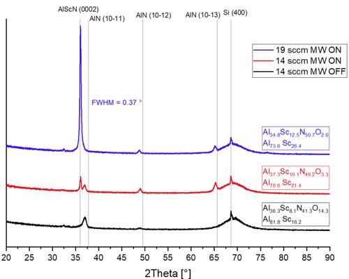
Many parameters can be adjusted in the plasma discharge to modify the samples properties. In this work, the most important one was the choice of the nitrogen flow, which determines weither the coating is going to be a metal or a ceramic material. Another process optimization was to combine the HiPIMS system with microwave (MW) electron cyclotron resonnance (ECR) plasma sources. This solution remains actually unexplored in the litterature and shows promising results, which could lead to a publication in thin films research journals. As observed on Fig. 1, these parameters have a strong influence on coating's atomic structure.
Thin films properties
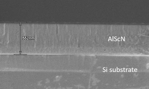
For appreciable film quality, the crystalline network should be dense and oriented in the (002) direction. Fig.1 shows the X-ray diffractogram of three different films, with the blue line corresponding to a deposition with optimized parameters. The sharp and narrow peak from the blue signal line at 2 Theta = 36 ° translates a strong preferiential orientation of the atomic structure in the desired piezolectric phase. From this result, it is expected to observe a significant increase in piezoelectric coefficient for this material. As XRD analysis of oriented films requires a solid understanding of the technique and deep analysis characterizing atomic structure was a major part of this work. On Fig.2, the AlScN layer (550 nm) presents non-columnar and high density structure.

